This is never going to be a complete guide on how to debug your build, but rather a collection of suggestions and observations on the subject. I’m assuming we’re working with non-lethal voltages typical for most stompboxes, i.e. in the region up to about +18V. Special care needs to be taken when working on high voltages and this won’t be covered here.
I welcome any corrections and suggestions on how to make this resource better. Let me know.
Keys to success:
- Work systematically – It’s a good idea to keep a print-out of the layout in front of you and mark off components etc. as you check them. The corresponding schematic can also help if you need to do something like tracing the audio path from input to output.
- Be patient – Sometimes it helps to put your work away and look at it with fresh eyes the next day.
- Sit back and consider the problem – This is often easier when you gain more experience, but you can almost always use logic and deduction to narrow the scope of the problem. Does everything work except the tone pot? Start by checking the pot, the pot wiring and the components immediately connected to where the pot wires connect to the board.
Visual inspection:
- Trace cuts – Flip the circuit board so you’re looking at the copper trace side. Make sure you’ve got the correct number of traces and that they’re at the correct spot (all layouts should have a trace cut count). Remember that the trace cuts on the layout are mirrored when you look at the trace side of the board. Note that there’s usually several trace cuts underneath ICs, and a layout usually also has a list of hard-to-spot trace cuts that are hidden underneath other components. Also make sure none of your trace cuts are incomplete, still providing a conductive path. Performing these checks right when you start, before you solder any components, is good practice and will eliminate a few problems down the road.
- Jumpers – All layouts have a jumper count; make sure you haven’t missed one (some might be partially or completely covered by an IC socket). It’s also easy to misplace a jumper or have it too short/long by one hole.
- Resistors/capacitors – Like jumpers make sure you haven’t forgotten or misplaced any. Also check that you’ve used the correct value. It’s easy to pick a resistor that’s 10x off because of the similarity in color coding. There’s plenty of good phone apps that can help you with the resistor and capacitor coding if you haven’t learned them by heart yet.
- Electrolytic capacitors – With electrolytics you also have to observe the polarity (unless you’re dealing with bi-polar/non-polar ones, but that’s quite rare). Most radial electrolytics will have an indicator showing you the negative side. Electrolytics on the layouts are indicated by a shaded band for the negative side, but I’ve also added a “+” indicator to make it easier (note that on some of the older layouts you’ll find a “+” on the shaded side; always go with the “+” indication).
- Tantalum electrolytics – Same as with the regular electrolytics except the component often has markings indicating the anode/positive leg instead. These are also quite fragile and susceptible to over-heating, so you have to be more careful not to damage them.
- Diodes – With these you have to observe the polarity. Most diodes come with a band indicating the cathode/negative side, which you should match against the diode on the layout. As with most semi-conductors they’re also a lot less forgiving of over-heating.
- Transistors – Make sure you’ve got the pinout right; this may differ between manufacturers. The illustrated transistor orientation on the layout may or may not be correct, but all layouts have a note specifying what the pinout should be. Find the datasheet of your specific transistor (google works) and match the pinout according to the note on the layout. (A good reason why you should use sockets for your transistors).
- ICs – Observe the orientation of the IC and that you’ve used the correct version (e.g. TL072 and not TL071). Make sure all the IC legs are properly inserted into the IC socket and not bent to the side.
- Solder bridges – Kind of self-explanatory, you’re looking for solder bridges between adjacent tracks or across trace cuts. It might be a good idea to touch up any border-line cases, or perhaps redo the joint altogether (solder sucker and new solder, less of it this time). While it’s not an elegant solution carefully running a knife along each of the lengths between the tracks could work; even a tiny solder bridge barely visible with a magnifying glass is enough to cause an electrical connection and throw your circuit off. And finally, the continuity tester on your DMM is great at finding adjacent tracks that are bridged, just keep in mind that sometimes they -should- (e.g. jumpers, diodes and very small resistors).
- Cold solder joints – This is another common one. You’ll hear people saying that a healthy joint looks shiny and a dull one is a potential problem. This is probably true for old school lead-solder, but I use the lead-free stuff and all my joints end up looking dull no matter what, so keep that in mind. If you look closely you can most likely spot any joints that look suspicious, but your DMM continuity tester will also be of help here. Re-flowing the joint in question is often enough to solve the problem.
Checking voltages:
This can be a great help in getting closer to the problem, but there might be some additional thinking required too. Remember that you have to power the circuit in order to get anything meaningful out of this.
- Make sure you’ve got a healthy battery or power source before starting.
- When applying power to the circuit, if the only thing happening is a component or the battery becoming hot you probably have a short somewhere and you should immediately turn the power off. Use other means of finding the problem, a visual inspection perhaps.
- All voltage readings are performed relative to ground so clip your black DMM probe here to free up one of your hands.
- You usually only read the voltages off of active components, i.e. transistors and ICs.
- Ideally you’ll have a full chart of expected voltages at every pin on the circuit, but even lacking this there’s a minimum of things you could verify.
- All ICs require a +V and a ground connection; look up the datasheet to locate the correct pins. You’d expect the IC +V pin to be at- or close to the +V your feeding the circuit, and the IC ground pin to read at most a few mV.
- Some ICs run at +5V and not the typical +9V, in which case you’re likely to also have a voltage regulator in your circuit (78L05 or similar; looks like a transistor). Look up the voltage regulator datasheet of your specific manufacturer (these reportedly often differ in pinouts) and make sure you’ve got the pinout correct according to the layout. Now you’d expect to read +V on one of the pins, ground on one, and then +5V on the last one.
- A lot of opamps and dual opamps have their input and output pins sitting at a bias voltage of approx. 1/2 the +V, but this isn’t always the case.
- Keep in mind that all voltage readings are going to vary a bit from circuit to circuit depending on many factors. This is fine.
- If you -do- find one or more pins that are way off here’s when a little logical thinking will help a lot. A detailed breakdown of how to follow up is outside the scope of this document, but a closer inspection of components and tracks directly connected to the pins in question is probably a good idea. A schematic or the ability to trace the connections on the layout will likely be of use here.
Using an audio probe:
Here’s a nifty tool that can help you listen to your signal as it progresses through the circuit; R. G. Keen’s improved audio probe. You build this little thing, connect it to a small amp (ideally with a volume control), use the clip to connect to your circuit ground and touch the probe at various points on your circuit to hear what your signal sounds like at that point.
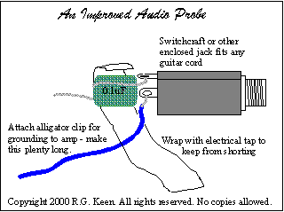
Now, just randomly “listening” to any point on your circuit isn’t likely to get you anywhere. What you need to do is keep a copy of both the schematic and the layout in front of you and slowly start to follow the audio path. You will need your circuit powered up and some kind of signal injected into the circuit input; you could keep strumming your guitar with one hand (or get your friend to do it for you), or maybe build a signal generator/sine wave oscillator of some kind to create a signal for you.
With everything set up start by verifying that you can probe and hear your signal at the “input” of your circuit. If you’re not getting an input signal debugging the rest of the circuit is moot; look at your setup, switch wiring etc. Once you’re getting a signal at “input” you start probing the signal along the audio path of the circuit. Here’s where the schematic will help you identify exactly what the audio path on the layout is. Let’s say you follow the signal through an input capacitor and into the first opamp or transistor gain stage, and there’s no signal at the gain stage output; you’ve just potentially discovered where the problem is (now’s the time to look for mistakes near that opamp stage or maybe verify the IC is getting power).
This can be a very powerful debugging tool for some circuits, but it can also be a great way to adjust the bias on those JFET preamp emulator circuits with all those trim pots (start probing the signal on the first JFET output (drain pin typically) and adjust the trimmer until you can hear a nice, beefy output signal, then continue to the next JFET gain stage, and so on).
Sorry you’re having trouble steve. The schematic calls for low current LEDs; perhaps the 5mm ones are a bit power hungry? Also, you’re using red LEDs (other LEDs have different voltage drops and may not work). And finally, you’re using the low current diffused kind, and not the ultra-bright ones?
I built the Easy vibe. I am getting no illumination of any LEDs. I have double checked the component layout and it is correct. The only substitutions I have made are TL074 for the ICs and 5mm LED instead of 3mm. The LDRs are 250mw 250V Peak 12K Ohm Max Light 1M Ohm MIN Dark. When I check the input voltage at the back of the power jack it is oscillating between .8v and 1.9v. The power supply unplugged gives a solid 9v. thx
Thank you very much Harald for your comments. It has taken almost a year, but I have now been able to build several working circuits. I found that my biggest issue was my cuts. The cuts were not always completely cutting off voltage across the board. I also had an issue with small pieces of copper running across the tracks. I re built the zombie chorus and it sounds awesome!! Thanks again Harald I love the site.
Hi Eric,
This one is tricky. It can be any number of things, really, but the likelihood that it’s a small mistake, be it a solder bridge or a missing component is fairly high. I suggest you check out the tips here in the debugging section, and if you feel it’s a bit over your head then maybe try a simpler circuit to give yourself a confidence boost as well as some “time off” from this circuit (often works wonders).
Hope that helps, at least a little bit.
Harold thanks so much for the great website. I am very new to pedal building and I just recently built the Zombie Chorus. The issue I have is when I turn it on, it doesn’t sound much different than my normal clean tone. The volume doesn’t change and adjusting Rate and/or Speed doesn’t seem to change anything. Do you have any suggestions.
Thanks again.
Hi Brando,
I haven’t got a deciphering table for pot tapers as these are, I think, pretty widely accepted. A = audio/log, B = linear, C = reverse audio/log.
When it comes to the capacitors the main difference is actually what you can afford and what you can physically fit on the circuit board. You typically find ceramic and mica capacitors occupying the picofarad (pF) space. Film capacitors (polyester, polypropylene etc.) is the logical choice in the nanofarad space (nF), and when you get to microfarads (uF) the film caps will become very large and expensive, so electrolytics take over. From an audio perspective film caps are generally referred to as sounding better, with mica caps for the small values (though some argue ceramics are just as good here).
Hope that will be of some help! 🙂
Hi Harald, I’m just getting into pedal building. Is there a table or key you can recommend for deciphering the potentiometer taper codes used in your layouts? Also, is there a way to know if a layout calls for electrolytic, film, ceramic, or silver mica capacitor?
Thank you for any help you can give!
Daniel afraid not. It could be a whole lot of things. Have you gone over everything several times with a magnifying glass and made sure there’s no mistakes of any kind?
I tried to connect the blend 1, 2 wire to both the 1 and 2 lugs on the blend pot and do as you said but i’m still getting the same problem. I have to strum the guitar really hard to hear anything and for some reason once I flick the vibrato switch on I can hear the guitar again. Do you have any idea on what’s going wrong here? Thanks for you help
Hi Daniel. Not sure about the transistor substitute, but I can tell you about the wiring at least.
It’s quite straight forward; you wire the Blend pot to the circuit as specified (lug #3 and lugs #1/#2 combined), then you wire the Bass switch lug #1 to the circuit board as specified. Lastly, you wire the Bass switch lug #2 directly to the Blend pot lugs #1/#2 (or to the board next to the Blend 1, 2 label if you prefer). There’s an off-board wiring list in the lower right-hand part of most of my layouts, and on this particular one it consists of just “Bass SW 2 -> Blend 1, 2”.
Hope that helps 🙂
Hi Harald.
I recently made a Boss Ce-2 w/mods and I replaced the 2N5088 transistors with
BC337. The circuit works except you have to turn the amp up really loud to hear it. Also i’m not sure how to wire up the blend pot with the bass switch. Any ideas on what’s going on here? Thanks
Yes. That’s correct, Cory.
On the Scrambler layout does “Blend 2-> Output” mean that Blend 2 goes to the circuit output on the 3DPT?
Thanks
Hi Cory. Sorry you’re not getting it to work properly.
Don’t worry, there isn’t any R8 and there isn’t supposed to be one either. And the C3 re-orientation is indeed reflected in the layout.
The diodes could have been damaged by heat (as could the transistors), but you’re saying you’re not even getting the indicator LED to light? Since the LED isn’t really connected to the board at all (goes straight from +V, via resistor to 3PDT and then to ground) I’m thinking it’s either going to be your off-board wiring (LED oriented correctly?) or something on the board is shorting +V to ground or similar (have you checked that you’ve got a good power source?). In short, there’s very little on the circuit board that could prevent that LED from glowing other than ruining/hijacking your +V source.
I am making the Ampeg Scrambler and have it all wired but get no LED and when it is switched on there is just a constant hum. I have checked my wiring and traces so I assume it is the board. Is there supposed to be a “R8”? Also is the reorientation of “C3” represented on the layout or does it still need to be switched around? Lastly could the diodes have been damaged by heat and therefore opening the circuit? Thank you.
I might, but high voltage stuff isn’t what this site is mainly about, at least at present.
Thank you, Harald..now I can start building your excellent CMOS vero layouts without fear 🙂 Also, would it be possible for you to publish a section on safety precautions to be followed when dealing with circuits that involve tubes and/or high voltages ?
Regards, and many thanks,
Jishnu
Hi Jishnu, good questions and I’ll have to see where I can put them in.
To give you an answer I think the CMOS and static electricity risk is a bit overrated. I’ve never had one go bad on me yet (knock on wood) and I haven’t been super careful handling them. I try to keep all semi-conductors, be it ICs, transistors or diodes, stored either in anti-static bags or attached to anti-static foam pieces.
When it’s time to use one in a circuit I always solder in an appropriately sized socket instead of the transistor/IC itself (the exception here is diodes).
Excellent stuff, Harald…although I have a query – could you give some tips on how to store, handle and solder ICs – specifically CMOS ICs, which I’ve heard are static sensitive…what precautions should I take whilst working with them?
Thanks and regards,
J.
This is very, very useful. I don’t think I have to tell you why.